A version of this chapter which is updated more frequently than the
yearly AO update of the Technical Description can be found at:
http://www.astro.isas.jaxa.jp/![]() tsujimot/td_xis.pdf.
tsujimot/td_xis.pdf.
The X-ray Imaging Spectrometer (XIS)7.1 is composed of four units of X-ray cameras (Fig. 7.1). These employ X-ray sensitive Si charge-coupled devices (CCDs) similarly to those used in the ASCA SIS, Chandra ACIS, XMM-Newton EPIC, and Swift XRT. In the photon counting mode, X-ray CCD detectors have imaging-spectroscopic capability. In each pixel of a CCD array, an incident X-ray photon is converted into a charge cloud with a total charge proportional to the energy of the absorbed X-ray. The charge is then shifted from one pixel to the next toward the gate of an output transistor by applying a time-varying electrical potential. This results in a voltage level (often referred to as ``pulse height'') proportional to the energy of the X-ray photon.
The four sensors are named XIS0, 1, 2 and 3. The CCDs are each placed at the focal plane of a dedicated X-Ray Telescope. The four X-Ray Telescope modules are called XRT-I0, XRT-I1, XRT-I2, and XRT-I3.
Each CCD camera has a single CCD chip with an array of 1024 ![]() 1024 pixels, covering an
1024 pixels, covering an
![]() region. Each pixel is
24
region. Each pixel is
24![]() m
m ![]() 24
24![]() m, and the size of the CCD is 25mm
m, and the size of the CCD is 25mm
![]() 25mm. One of the sensors (XIS1) uses a back side
illuminated (BI) CCD, while the other three use a front side
illuminated (FI) CCD. The XIS was developed and has been maintained
jointly by Japan and the United States, with participating
organizations including MIT, ISAS, Kyoto University, Osaka University,
Rikkyo University, Ehime University, Miyazaki University, Kogakuin
University, and Nagoya University.
25mm. One of the sensors (XIS1) uses a back side
illuminated (BI) CCD, while the other three use a front side
illuminated (FI) CCD. The XIS was developed and has been maintained
jointly by Japan and the United States, with participating
organizations including MIT, ISAS, Kyoto University, Osaka University,
Rikkyo University, Ehime University, Miyazaki University, Kogakuin
University, and Nagoya University.
The XIS has been operated successfully since the launch in July 2005. The detector performance changes both continuously and discontinuously. One of the causes for discontinuous changes is the unavoidable occurrence of micro-meteorite hits in orbit. Such an event in November 2006 made the entire XIS2 dysfunctional. Another one in June 2009 caused a part of the XIS0 to be dysfunctional. Yet another one in December 2009 hit the XIS1, but its scientific impact has been evaluated to be minimal. Section 7.12 discusses the anomalies caused by these events. Users need to be aware of possible discontinuous changes through web resources and Suzaku memos.
![\includegraphics[height=6.0in]{figures_xis/xis_config_v2}](img152.png)
|
A CCD has a gate structure on one of the surfaces to transfer the charge packets to the readout gate. The surface of the chip with the gate structure is called the ``front side''. A front side illuminated CCD (FI CCD) detects X-ray photons that pass through its gate structures, i.e., from the front side. Because of the additional photo-electric absorption at the gate structure, the low-energy quantum efficiency (QE) of the FI CCD is rather limited. Conversely, a back side illuminated CCD (BI CCD) receives photons from ``back,'' or the side without the gate structures. For this purpose, the undepleted layer of the CCD is completely removed in the BI CCD, and a thin layer to enhance the electron collection efficiency is added in the back surface. A BI CCD retains a high QE even in a sub-keV energy band because of the absence of the gate structure on the photon detection side. However, a BI CCD tends to have a slightly thinner depletion layer, and the QE is therefore slightly lower in the high energy band. The decision to use only one BI CCD and three FI CCDs was made because of the slight additional risk involved in the new BI technology and the need to balance the overall efficiency for low and high energy photons.
Fig. 7.2 provides a schematic view of the XIS system.
The Analog Electronics (AE) drive the CCD and processes its data.
Charge clouds produced in the exposure area in the CCD are transferred
to the Frame Store Area (FSA) after the exposure according to the
clocks supplied by the AE. The AE reads out data stored in the FSA
sequentially, amplifies the data, and performs the analog-to-digital
conversion. The AE outputs the digital data into the memory named
Pixel RAM in the Pixel Processing Units (PPU). Subsequent data
processing is done by accessing the Pixel RAM. To minimize the thermal
noise, the sensors need to be kept at
![]() C during
observations. This is accomplished by thermo-electric coolers (TECs),
controlled by TEC Control Electronics, or TCE. The AE and TCE are
located in the same housing, and together, they are called the
AE/TCE. Suzaku has two AE/TCEs. AE/TCE01 is used for XIS0 and 1, and
AE/TCE23 is used for XIS2 and 3. The digital electronics system for
the XIS consists of two PPUs and one Main Processing Unit (MPU); PPU01
is associated with AE/TCE01, and PPU23 is associated with
AE/TCE23. The PPUs access the raw CCD data in the Pixel RAM, carry out
event detection, and send event data to the MPU. The MPU edits and
packets the event data, and sends them to the satellite's main digital
processor.
C during
observations. This is accomplished by thermo-electric coolers (TECs),
controlled by TEC Control Electronics, or TCE. The AE and TCE are
located in the same housing, and together, they are called the
AE/TCE. Suzaku has two AE/TCEs. AE/TCE01 is used for XIS0 and 1, and
AE/TCE23 is used for XIS2 and 3. The digital electronics system for
the XIS consists of two PPUs and one Main Processing Unit (MPU); PPU01
is associated with AE/TCE01, and PPU23 is associated with
AE/TCE23. The PPUs access the raw CCD data in the Pixel RAM, carry out
event detection, and send event data to the MPU. The MPU edits and
packets the event data, and sends them to the satellite's main digital
processor.
To reduce contamination of the X-ray signal by optical and UV light,
each XIS has an Optical Blocking Filter (OBF) located in front of it.
The OBF is made of polyimide with a thickness of 1000Å, coated
with a total of 1200Å of aluminum (400Å on one side and
800Å on the other side). To facilitate the in-flight calibration
of the XISs, each CCD sensor has two ![]() Fe calibration sources
7.2. These sources are
located on the side wall of the housing and are collimated in order to
illuminate two corners of the CCDs. They can easily be seen in two
corners of each CCD. A small number of these X-rays scatter onto the
entire CCD.
Fe calibration sources
7.2. These sources are
located on the side wall of the housing and are collimated in order to
illuminate two corners of the CCDs. They can easily be seen in two
corners of each CCD. A small number of these X-rays scatter onto the
entire CCD.
The XIS had unexpectedly large contamination on the OBF from some
material in the satellite. This reduced the low-energy efficiency of
the XIS significantly. We monitor the contamination thickness by
observing the calibration targets (e.g., 1E0102![]() 72,
RXJ1856.5
72,
RXJ1856.5![]() 3754) regularly. This effect is included in the response
matrices. Details of the contamination are explained in
section 7.8.
3754) regularly. This effect is included in the response
matrices. Details of the contamination are explained in
section 7.8.
It is known that the CCD performance gradually degrades in space due to the radiation damage. This is because charge traps are produced by cosmic rays and are accumulated in the CCD. One of the unique features of the XIS is the capability to inject small amounts of charge to the pixels. The charge injection is quite useful to fill the charge traps periodically, and to make them almost harmless. This method is called the spaced-row charge injection (SCI), and the SCI has been adopted as a standard method since AO-2 to cope with the increase of the radiation damage (Uchiyama et al. 2009). The charge injection capability is also used to measure the charge transfer efficiency (CTE) of each CCD column in the case of the no-SCI mode (Ozawa et al., 2009; Nakajima et al., 2008). Details of the charge injection are explained in section 7.6.
A single XIS CCD chip consists of four segments (marked A, B, C and D in Fig. 7.2) and correspondingly has four separate readout nodes. Pixel data collected in each segment are read out from the corresponding readout node and sent to the Pixel RAM. In the Pixel RAM, pixels are given RAW X and RAW Y coordinates for each segment in the order of the readout, such that RAW X values are from 0 to 255 and RAW Y values are from 0 to 1023. These pixels in the Pixel RAM are named active pixels.
In the same segment, pixels closer to the read-out node are read-out faster and stored in the Pixel RAM faster. Hence, the order of the pixel read-out is the same for segments A and C, and for segments B and D, but different between these two segment pairs, because of the different locations of the readout nodes. In Fig. 7.2, numbers 1, 2, 3 and 4 marked on each segment and the Pixel RAM indicate the order of the pixel read-out and the storage in the Pixel RAM.
In addition to the active pixels, the Pixel RAM stores the copied pixels, dummy pixels and H-over-clocked pixels (Fig. 7.2). At the borders between two segments, two columns of pixels are copied from each segment to the other. Thus these are named copied pixels. Two columns of empty dummy pixels are attached to the segments A and D. In addition, 16 columns of H-over-clocked pixels are attached to each segment.
Actual pixel locations on the chip are calculated from the RAW XY coordinates and the segment ID during ground processing. The coordinates describing the actual pixel location on the chip are named ACT X and ACT Y coordinates (Fig. 7.2). It is important to note that the RAW XY to ACT XY conversion depends on the on-board data processing mode (see section 7.4).
When a CCD pixel absorbs an X-ray photon, the X-ray is converted to an electric charge, which in turn produces a voltage at the analog output of the CCD. This voltage (``pulse height'') is proportional to the energy of the incident X-ray. In order to determine the true pulse height corresponding to the input X-ray energy, it is necessary to subtract the dark levels and correct possible optical light leaks.
Dark levels are non-zero pixel pulse heights caused by leakage currents in the CCD. In addition, optical and UV light might enter the sensor due to imperfect shielding (``light leak''), producing pulse heights that are not related to X-rays. The analysis of the ASCA SIS data, which utilized the X-ray CCD in photon-counting mode for the first time, showed that the dark levels were different from pixel to pixel, and the distribution of the dark level did not necessarily follow a Gaussian function. On the other hand, light leaks are considered to be rather uniform over the CCD.
For the Suzaku XIS, the dark levels and the light leaks are calculated separately in the normal mode. The dark levels are defined for each pixel and are expected to be constant for a given observation. The PPU calculates the dark levels in the Dark Initial mode (one of the special diagnostic modes of the XIS); those are stored in the Dark Level RAM. The average dark level is determined for each pixel, and if the dark level is higher than the hot-pixel threshold, this pixel is labeled as a hot pixel. The dark levels can be updated by the Dark Update mode, and sent to the telemetry by the Dark Frame mode. The analysis of the ASCA data showed that the dark levels tend to change mostly during the SAA passage of the satellite. The Dark Update mode may be employed several times a day after the SAA passage.
Hot pixels are pixels which always output pulse heights larger than the hot-pixel threshold even without input signals. Hot pixels are not usable for observations, and their outputs have to be disregarded during scientific analysis. The XIS detects hot pixels on-board by the Dark Initial/Update mode, and their positions are registered in the Dark Level RAM. Thus, hot pixels can be recognized on-board, and they are excluded from the event detection processes. It is also possible to specify the hot pixels manually. However, some pixels output pulse heights larger than the threshold intermittently. Such pixels are called flickering pixels. It is difficult to identify and remove the flickering pixels on board. They are inevitably output to the telemetry and need to be removed in scientific analyses, for example by using the FTOOLS sisclean. Flickering pixels sometimes cluster around specific columns, which makes them relatively easy to identify.
The light leaks are calculated on board with the pulse height data
after subtraction of the dark levels. A truncated average is
calculated for ![]() pixels (this size was
pixels (this size was ![]() before January 18, 2006) in every exposure and its running average
produces the light leak. In spite of the name, light leaks do not
represent in reality optical/UV light leaks to the CCD. They mostly
represent fluctuation of the CCD output correlated to the variations
of the satellite bus voltage. The XIS has little optical/UV light
leak, which is negligible unless the bright Earth comes close to the
XIS field of view.
before January 18, 2006) in every exposure and its running average
produces the light leak. In spite of the name, light leaks do not
represent in reality optical/UV light leaks to the CCD. They mostly
represent fluctuation of the CCD output correlated to the variations
of the satellite bus voltage. The XIS has little optical/UV light
leak, which is negligible unless the bright Earth comes close to the
XIS field of view.
The dark levels and the light leaks are merged in the Parallel-sum (P-Sum) mode, so the Dark Update mode is not available in the P-Sum mode. The dark levels, which are defined for each pixel as the case of the normal mode, are updated every exposure. It may be considered that the light leak is defined for each pixel in the P-Sum mode.
The main purpose of the on-board processing of the CCD data is to reduce the total amount of data transmitted to the ground. For this purpose, the PPU searches for a characteristic pattern of the charge distribution (called an event) in the pre-processed (post- dark level and light leak subtraction) frame data. When an X-ray photon is absorbed in a pixel, the photo-ionized electrons can spread into at most four adjacent pixels.
An event is recognized when a pixel has a pulse height which is
between the lower and the upper event thresholds and is larger than
those of eight adjacent pixels (e.g., it is the peak value in the
![]() pixel grid). In the P-Sum mode, only the horizontally
adjacent pixels are considered. The copied and the dummy pixels ensure
that the event search is enabled on the pixels at the edges of each
segment. The RAW XY coordinates of the central pixel are considered
the location of the event. Pulse-height data for the adjacent
pixel grid). In the P-Sum mode, only the horizontally
adjacent pixels are considered. The copied and the dummy pixels ensure
that the event search is enabled on the pixels at the edges of each
segment. The RAW XY coordinates of the central pixel are considered
the location of the event. Pulse-height data for the adjacent ![]() square pixels (or three horizontal pixels in the P-Sum mode)
are sent to the Event RAM as well as the pixel location.
square pixels (or three horizontal pixels in the P-Sum mode)
are sent to the Event RAM as well as the pixel location.
The MPU reads the Event RAM and edits the data to the telemetry
format. The amount of information sent to the telemetry depends on the
editing mode of the XIS. All the editing modes (in the normal mode,
see section 7.5) are designed to send the pulse heights
of at least four pixels of an event to the telemetry, because the
charge cloud produced by an X-ray photon can spread into at most four
pixels. Information of the surrounding pixels may or may not be output
to the telemetry depending on the editing mode. The ![]() mode
outputs the most detailed information to the telemetry, i.e., all 25
pulse-heights from the
mode
outputs the most detailed information to the telemetry, i.e., all 25
pulse-heights from the ![]() pixels containing the event. The
size of the telemetry data per event is reduced by a factor of two in
the
pixels containing the event. The
size of the telemetry data per event is reduced by a factor of two in
the ![]() mode, and another factor of two in the
mode, and another factor of two in the ![]() mode. Details of the pulse height information sent to the telemetry
are described in the next section.
mode. Details of the pulse height information sent to the telemetry
are described in the next section.
There are two different kinds of on-board data processing modes. The Clock modes describe how the CCD clocks are driven, and determine the exposure time, the exposure region, and the time resolution. The Clock modes are determined by a program (``micro-code'') loaded into the AE. The Editing modes specify how detected events are edited, and determine the format of the XIS data telemetry. The Editing modes are determined by the digital electronics.
In principle, each XIS sensor can be operated with different mode
combinations. However, we expect that most observations will use all
three sensors7.3 in the Normal 5
![]() 5 or 3
5 or 3 ![]() 3 mode (without the Burst or Window options).
Other modes are useful for bright sources (when pile-up or telemetry
limitations are a concern) or if a higher time resolution (
3 mode (without the Burst or Window options).
Other modes are useful for bright sources (when pile-up or telemetry
limitations are a concern) or if a higher time resolution (![]() 8s) is
required.
8s) is
required.
There are two kinds of Clock modes in the XIS, the Normal and the Parallel-Sum (P-sum) mode. Furthermore, two options (the Window and the Burst options) may be used in combination with the Normal mode. However, see section 7.5.3 for restrictions using the Parallel-Sum mode.
Table 7.1 indicates how the effective area and exposure time are modified by the Burst and the Window options.
| Option | Effective area | Exposure time |
| (nominal:
|
(in 8s period) | |
| None |
|
8s |
| Burst |
|
|
| Window | 2s |
|
| 1s |
||
| Burst & Window | ||
| Note: |
||
In the Normal Clock mode, the Window and the Burst options can modify the effective area and exposure time, respectively. The two options are independent, and may be used simultaneously. These options cannot be used with the P-Sum Clock mode.
The Window width can be 128 pixels (1/8 Window). However, a significant fraction of the source photons may be lost due to the tail of the XRT point spread function. Furthermore, the fractional loss may be modulated by the attitude fluctuation of the satellite, which is synchronized with the orbital motion of the satellite. Thus the XIS team do not recommend the 1/8 Window option.
One of the disadvantages of the Window option is that the X-rays from
the calibration sources ![]() Fe are out of the Window. This makes it
difficult to check the gain and the energy resolution of the XIS.
Fe are out of the Window. This makes it
difficult to check the gain and the energy resolution of the XIS.
|
We show in Fig. 7.3 the time sequence of exposure, frame-store transfer, CCD readout, and storage to the Pixel RAM (in PPU) in the normal mode with or without the Burst/Window option.
Editing modes may be divided into two categories, observation modes
and diagnostics modes. We describe here mainly the observation modes.
General users usually do not need to analyze the data of the
diagnostic modes. Among the observation modes, three modes (![]() ,
, ![]() , and
, and ![]() ) are usable in the Normal Clock
mode, and only the Timing mode can be specified in the P-Sum mode.
) are usable in the Normal Clock
mode, and only the Timing mode can be specified in the P-Sum mode.
Please note that guest observers cannot specify the Editing mode for their observations; the Suzaku operation team selects the Editing mode by considering the counting rate and the telemetry limit.
Observation Modes
We show in Fig. 7.4 the pixel pattern whose pulse height
or 1-bit information is sent to the telemetry. We do not assign grades
to an event on board in the Normal Clock mode. This means that a dark
frame error, if present, can be corrected accurately during the ground
processing even in the 2 ![]() 2 mode. The definition of the grades
in the P-Sum mode is shown in Fig. 7.5.
2 mode. The definition of the grades
in the P-Sum mode is shown in Fig. 7.5.
No significant difference has been found so far between the ![]() and
and ![]() modes. However, the
modes. However, the ![]() mode is slightly
different from the
mode is slightly
different from the ![]() or
or ![]() mode. The difference is
produced during the CTE correction in the ground processing. Because
the pulse height information is limited in the
mode. The difference is
produced during the CTE correction in the ground processing. Because
the pulse height information is limited in the ![]() mode, some
of the CTE corrections cannot be applied to the
mode, some
of the CTE corrections cannot be applied to the ![]() mode
data. This causes a slight difference in the gain of the
mode
data. This causes a slight difference in the gain of the ![]() mode data. As of August 2009, the gain difference has been measured,
and the XIS software (xispi) takes the difference into
consideration. However, the gain adjustment is optimized at the XIS
nominal position and a slight gain difference of about 5 eV at 6 keV
can be seen at off-axis positions. The
mode data. As of August 2009, the gain difference has been measured,
and the XIS software (xispi) takes the difference into
consideration. However, the gain adjustment is optimized at the XIS
nominal position and a slight gain difference of about 5 eV at 6 keV
can be seen at off-axis positions. The ![]() mode is employed
only when a bright source is observed (see tables 7.9
and 7.10). Those who plan to observe a bright source
should be aware of these systematics in the
mode is employed
only when a bright source is observed (see tables 7.9
and 7.10). Those who plan to observe a bright source
should be aware of these systematics in the ![]() mode. The
mode. The ![]() mode is not used in the BI CCD (XIS1), because a relatively
small CTE in the BI CCD produces significant calibration difference
from the
mode is not used in the BI CCD (XIS1), because a relatively
small CTE in the BI CCD produces significant calibration difference
from the ![]() and the
and the ![]() modes.
modes.
Note on the Timing Mode
From AO-5 on, the Timing mode can be used for a restricted numbers of observations. The total exposure of the Timing mode must be less than 5%. However, the calibration accuracy of the Timing mode is worse compared to the Normal mode. Therefore, those who consider using the Timing mode should demonstrate the feasibility of their observations under the larger calibration inaccuracies described below.
The Timing mode is available only for the XIS3. There are comparably large numbers of hot/flickering pixels in the BI CCD, which are difficult to remove completely on board. The remaining hot/flickering pixels are found to fill the telemetry easily, since a single hot pixel can produce 1024 events in 8s in the Timing mode. Due to this telemetry usage by hot/flickering pixels, we cannot use the Timing mode for the BI CCD. Note that this does not happen in the Normal mode. The FI CCDs have only a small number of hot/flickering pixels, although some of them need to be removed during the data analysis.
Since only one dimensional information is available in the Timing mode, the distinction between X-ray and non-X-ray events becomes inaccurate. This means that the Timing mode has a significantly higher non-X-ray background than the Normal mode. Preliminary analyses showed that the non-X-ray background in the Timing mode is one or two orders of magnitude larger than in the Normal mode. Because the available data are limited, its detailed behavior, e.g. dependence on the cut-off rigidity, is not known.
The in-flight calibration of the Timing mode is taken into account in the data processing. The calibration accuracy will not reach the level achieved for the Normal mode, because (1) the Spaced-row Charge Injection (SCI) is not available on board and (2) the CTI correction is difficult in the ground processing. Those who consider to use the Timing mode (or to analyze the Timing mode data) are advised to visit the Suzaku web pages for the latest calibration information.
Unavailability of the SCI or the CTI correction means that the energy
scale and resolution are significantly different from those of the
Normal mode. In addition, the effective area of the CCDs may change in
the Timing mode: even a small number of hot pixels produces a
relatively large dead area in the CCD, which reduces the effective
area. This reduction could be time dependent, because some of the hot
pixels often disappear and reappear. The nominal time resolution in
the Timing mode is 7.8ms, but this depends on the image size of the
X-ray source. If the X-ray image is much larger than 128 pixels
(![]() 2 arcmin) along the Y-address, the time resolution may become
worse than 7.8ms. Because the Y-address represents the photon
arrival time in the Timing mode, the image extension (in the
Y-direction) works as a low-pass filter. This means that, even for a
point source, some signal is leaked to the adjacent time bins due to
the tail of the XRT PSF. Therefore, the frequency response is somewhat
reduced near the Nyquist frequency of the nominal time resolution of
7.8ms.
2 arcmin) along the Y-address, the time resolution may become
worse than 7.8ms. Because the Y-address represents the photon
arrival time in the Timing mode, the image extension (in the
Y-direction) works as a low-pass filter. This means that, even for a
point source, some signal is leaked to the adjacent time bins due to
the tail of the XRT PSF. Therefore, the frequency response is somewhat
reduced near the Nyquist frequency of the nominal time resolution of
7.8ms.
|
|
Diagnostic Modes
Besides the observation modes explained above, the XIS instrument has several diagnostic modes, the Frame mode, the Dark Initial mode, the Dark Update mode, and the Dark Frame mode. The Frame mode simply dumps the raw CCD data to the telemetry. This mode may be useful for the health check of the CCD. Other modes are used primarily in determining/checking the dark levels. The Dark Init mode is employed when the Burst/Window options are changed. The Dark Update mode is used just after the SAA passage to update the hot pixel list on board. It is unlikely that those would be used by guest observers.
Three kinds of discriminators, the area, the grade and the class discriminators, can be applied during the on-board processing. The grade discriminator is available only in the Timing mode. The class discriminator was implemented after the launch of Suzaku and was used since January, 2006. In most cases, guest observers need not to change the default setting of these discriminators.
The class discriminator classifies the events into two classes,
``X-rays'' and ``others,'' and outputs only the "X-ray" class to the
telemetry when it is enabled. This class discriminator is always
enabled to reduce the telemetry usage of non-X-ray events. The
``other'' class is close to, but slightly different from the ASCA
grade 7. When the XIS points to a blank sky, more than 90% of the
detected events are particle events (mostly the ASCA grade 7). If we
reject these particle events on board, we can make a substantial
saving in the telemetry usage. This is especially useful when the data
rate is medium or low. The class discriminator realizes such a
function in a simple manner. When all the eight pixels surrounding the
event center exceed the Inner Split Threshold, the event is classified
as the ``other'' class, and the rest of the events as the ``X-ray''
class. With such a simple method, we can reject more than three
quarters of the particle events. The class discriminator works only
for the ![]() and
and ![]() modes. It is not available in
the
modes. It is not available in
the ![]() mode and the timing mode.
mode and the timing mode.
The area discriminator is used when we want to reject some (or most) of the frame data from the event extraction. The discriminator works on the Pixel RAM. When the discriminator is enabled, a part of the Pixel RAM is not used for the event extraction. This may be useful when a bright source is present in the XIS field of view other than the target source. If we set the discrimination area to include only the bright source, we can avoid outputting unnecessary events to the telemetry. Only a single, rectangular area can be specified in a segment for discrimination. Either the inside or the outside of the area can be rejected from the event extraction. Note that the area discriminator works on the Pixel RAM, not on the physical area of the CCD. This is important when we apply the discriminator with the Window option.
The grade discriminator is only used in the timing mode. Any combination of the four grades can be selected to discriminate the grade for telemetry output.
Suzaku does not have the level discriminator, which was used in the ASCA SIS. The same function can be realized, however, by changing the event threshold.
X-ray CCD devices are subject to degradation in orbit. One of the outcomes is an increase of charge traps under the constant irradiation by cosmic rays in the space environment. This results in an increase of the charge transfer inefficiency (CTI), which leads to a degradation of the energy resolution.
|
The XIS has a functionality to precisely monitor and mitigate this
effect. For monitoring each sensor has ![]() Fe calibration sources
at two corners on the far side of the readout. For mitigation the
spaced-row charge injection (SCI) is implemented. Electrons are
injected artificially from one side of the chip and are read out along
with charges produced by X-ray events. The artificial charges are
injected periodically in space (every 54 rows;
Fig. 7.6). They fill up charge traps and thereby
alleviate the increase in CTI for charges by X-ray events
(Bautz et al., 2004).
Fe calibration sources
at two corners on the far side of the readout. For mitigation the
spaced-row charge injection (SCI) is implemented. Electrons are
injected artificially from one side of the chip and are read out along
with charges produced by X-ray events. The artificial charges are
injected periodically in space (every 54 rows;
Fig. 7.6). They fill up charge traps and thereby
alleviate the increase in CTI for charges by X-ray events
(Bautz et al., 2004).
Fig. 7.7 shows the long-term trend of the measured peak
energy and width of the Mn I K![]() line (5.9keV) from the
calibration sources. The peak energy decreases and the width increases
gradually. Both quantities are restored by applying the SCI.
line (5.9keV) from the
calibration sources. The peak energy decreases and the width increases
gradually. Both quantities are restored by applying the SCI.
|
The calibration of the spectroscopic performance of the XIS mainly consists of calibrating the energy gain and resolution. Regarding the energy gain, corrections for charge trails and for the CTI are performed.
For the energy resolution, the time dependence is modeled as
| (7.1) |
|
|
|
|
|
![\includegraphics[width=0.45\textwidth]{figures_xis/xis0_P_noseg}](img179.png)
![\includegraphics[width=0.45\textwidth]{figures_xis/xis1_P_noseg}](img180.png)
![\includegraphics[width=0.45\textwidth]{figures_xis/xis3_P_noseg}](img181.png)
|
The pulse height correction for the Normal mode with Window options is the same as that for the Normal mode with no option, except that they use different numbers of fast and slow charge transfers. Fast and slow transfers are used for reading out the imaging and frame store areas, respectively. They have different CTIs. For the Window options, the effective imaging area is limited, so the numbers of fast and slow transfers change. The CTI in each transfer is calibrated using calibration observations with the 1/4 Window option. This calibration is also applied to the 1/8 Window option.
Figure 7.12 shows the resulting gain using the Fe XXV
K![]() emission line, comparing the Normal mode with no option and
the Normal mode with the 1/4 Window option.
emission line, comparing the Normal mode with no option and
the Normal mode with the 1/4 Window option.
Figure 7.13 shows the ![]() Fe calibration source spectrum
taken with the 2.0s Burst option during an observation of GX
17
Fe calibration source spectrum
taken with the 2.0s Burst option during an observation of GX
17![]() 2. It has been modeled using the RMF for the Normal mode with no
option. There is no structure in the residuals, indicating that the
response is the same for the Normal mode with no option and with the
2.0s Burst option.
2. It has been modeled using the RMF for the Normal mode with no
option. There is no structure in the residuals, indicating that the
response is the same for the Normal mode with no option and with the
2.0s Burst option.
|
Fig. 7.14 shows the history of phenomenological gain of the P-sum data. Fig. 7.15 shows the energy resolution of a representative line in the soft and the hard band.
|
The calibration described above can be applied by using the xisrmfgen tool (Ishisaki et al., 2007).
In all modes the uncertainty of the gain and energy resolution calibration at the Si K edge remains large. Substantial efforts are currently being made to address this issue.
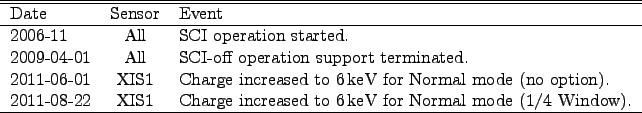
For XIS1 with the increased (6keV equivalent) charge injection (section 7.6), the long-term trend of the gain and of the energy resolution is not characterized yet. Therefore, their calibration uncertainty may be larger than for the original (2keV equivalent) charge injection.
The quantum efficiency below ![]() 2 keV has been decreasing since
launch due to accumulation of contaminating material on the optical
blocking filter (OBF) of each sensor. The OBF is cooler than other
parts of the satellite, thus is prone to contamination.
2 keV has been decreasing since
launch due to accumulation of contaminating material on the optical
blocking filter (OBF) of each sensor. The OBF is cooler than other
parts of the satellite, thus is prone to contamination.
The contaminant consists of several different materials with time-varying composition. The time dependence of the thickness and of the chemical composition of the contaminant at the XIS nominal position are monitored and calibrated, as well as the spatial dependence of the thickness across the field of view (Table 7.3).
The chemical composition is modeled phenomenologically with
time-varying columns of H, C, and O. This requires sufficient photons
between the C I and O I K edges at 0.28 and 0.53keV,
respectively. Regular observations of the super-soft isolated neutron
star RXJ1856.5![]() 3754 at the XIS nominal position are used for this
task. The BI spectra are fitted following the method described by
Burwitz et al. (2003) with additional absorption columns of H, C, and O
(Fig. 7.16). The composition derived from the BI
sensor at the XIS nominal position is applied to the FI sensors and
the other parts of the sensor.
3754 at the XIS nominal position are used for this
task. The BI spectra are fitted following the method described by
Burwitz et al. (2003) with additional absorption columns of H, C, and O
(Fig. 7.16). The composition derived from the BI
sensor at the XIS nominal position is applied to the FI sensors and
the other parts of the sensor.
|
The time dependence of the contamination thickness is modeled with
phenomenological functions, separately for each sensor. For this
purpose E0102![]() 72, a thermal supernova remnant in the Small
Magellanic Cloud, is observed regularly at the XIS nominal
position. Using the model by Plucinsky et al. (2008) the thickness of the
contaminants (mainly of O) is constraunde using the chemical
composition derived from the RXJ1856.5
72, a thermal supernova remnant in the Small
Magellanic Cloud, is observed regularly at the XIS nominal
position. Using the model by Plucinsky et al. (2008) the thickness of the
contaminants (mainly of O) is constraunde using the chemical
composition derived from the RXJ1856.5![]() 3754 observations (see
above).
3754 observations (see
above).
Figure 7.17 shows the evolution of the thickness. The thickness increased rapidly after launch for one year and continued to increase at a moderate pace thereafter. The monitoring frequency was decreased from once in three months to once in four months in 2011.
|
The spatial distribution of the contaminants is monitored and calibrated using regular observations of a part of the Cygnus Loop, a thermal supernova remnant. In addition atmospheric fluorescent K lines of N I and O I are used which illuminate the entire field of view when the telescope is oriented toward the day Earth.
The model of the spatial dependence assumes the radially symmetric
pattern (Koyama et al., 2007). The thickness at the center is normalized to
the value obtained from the E0102![]() 72 observations (see above) and
the chemical composition fixed to the value obtained from the
RXJ1856.5
72 observations (see above) and
the chemical composition fixed to the value obtained from the
RXJ1856.5![]() 3754 observations (see above). Different sensors have
different radial profiles (Figure 7.18).
3754 observations (see above). Different sensors have
different radial profiles (Figure 7.18).
|
The contamination calibration results are available through the ARF generation tool xissimarfgen (Ishisaki et al., 2007). The use of generic contamination models in the XSPEC package is discouraged (e.g., xisabs, xiscoabs, xiscoabh, xispcoab).
For proposal writers ARF files are provided that assume a contamination thickness extrapolated to the middle of the next AO cycle (Fig. 7.17).
It is known that the current time dependence model is starting to deviate from the observed data, especially for XIS0 and XIS3 (Fig. 7.19). The model will be updated in the near future.
[XIS0] |
All Suzaku XISs have low backgrounds, due to a combination of Suzaku's orbit and the instrumental design. The large effective area at the Fe K line band (comparable to the XMM-Newton PN) combined with this low background makes Suzaku a powerful tool for investigating high energy sources. The background originates from the cosmic X-ray background (CXB) combined with charged particles (the non-X-ray background or NXB). Currently, flickering pixels are a negligible component of the background. When observing the dark Earth (i.e., the NXB), the background rate in the 0.4-12keV band is 0.1-0.2counts/s in the FI CCDs and 0.3-0.6counts/s in the BI CCD. Note that these are the fluxes after the grade selection is applied with only the ASCA grades 0, 2, 3, 4, and 6 being selected. Fig. 7.20 shows the NXB spectra for each sensor.
![\includegraphics[width=0.8\textwidth]{figures_xis/fig1_9}](img193.png)
|
![\includegraphics[height=2.5in]{figures_xis/fig10_xis0}](img194.png)
![\includegraphics[height=2.5in]{figures_xis/fig10_xis1}](img195.png)
![\includegraphics[height=2.5in]{figures_xis/fig10_xis3}](img196.png)
![\includegraphics[height=2.5in]{figures_xis/fig10_dummy}](img197.png)
|
![\includegraphics[width=0.6\textwidth]{figures_xis/fig11}](img198.png)
|
There are also fluorescence features arising from the calibration sources as well as material in the XIS and XRTs. The Mn lines are due to scattered X-rays from the calibration sources. As shown in Table 7.4 they are almost negligible except for XIS0. The other lines are fluorescent lines from the material used for the sensor. Table 7.4 shows the current best estimates for the strength of these emission features, along with their 90% confidence errors.
The NXB is not uniform over the chip. Its flux tends to be slightly higher at larger ACTY as shown in Fig. 7.21. This is because some fraction of NXB is produced in the frame-store region. The fraction may be different between the fluorescent lines and the continuum. This causes slight difference in the ACTY dependence of the NXB.
The total flux of the NXB depends on the cut-off rigidity (COR) as shown in Fig. 7.22. This is expected as the NXB is produced by the charged particles, the flux of which is higher at lower COR. This means that, when we use the NXB database to subtract the background, we need to select the NXB for an appropriate range of COR values, which matches with the COR distribution of the on-source observation. For this purpose, the XIS FTOOL xisnxbgen can be used.
The count rate of the PIN upper discriminator (PIN-UD) in the HXD also correlates with the flux of the XIS NXB. Recent studies show the PIN-UD provides a slightly better reproducibility of the XIS NXB. The reproducibility of the NXB in the 5-12keV band is evaluated to be 3-4% of the NXB, when we use the PIN-UD as the NXB sorting parameter (Tawa et al. 2008).
When we estimate the telemetry usage of the background, we need to consider not only the X-ray grades (the ASCA grade 0, 2, 3, 4, 6) but also the non-X-ray grades (the ASCA grade 1, 5, 7). Although the class discriminator removes a large fraction of the non-X-ray background, we still have a non-negligible flux of the background. The background rate on the FI chips (including all the grades) is normally less than 10 counts/s and that of the BI CCD is less than 20 counts/s. These values represent the 90% upper limits of variations in the background count rates when the class discriminator is applied. These background rates are important when evaluating the possibility of telemetry saturation at low data rates (see section 7.10.4).
| Line | Energy | XIS0 | XIS1 | XIS2 | XIS3 |
| [keV] | [ |
[ |
[ |
[ |
|
| Al K |
1.486 | ||||
| Si K |
1.740 | ||||
| Au M |
2.123 | ||||
| Mn K |
5.895 | ||||
| Mn K |
6.490 | ||||
| Ni K |
7.470 | ||||
| Ni K |
8.265 | ||||
| Au L |
9.671 | ||||
| Au L |
11.51 |
![\includegraphics[width=0.8\textwidth]{figures_xis/pile-up}](img236.png)
|
The XIS is essentially a position-sensitive integrating instrument, with a nominal interval of 8s between readouts. If more than one photon strikes the same CCD pixel during the integration time, or one of its immediate neighbors, these cannot correctly be detected as independent photons; this is the phenomenon of photon pile-up. Here, the modest angular resolution of the Suzaku XRT is an advantage. However, photon pile-up can be a problem when observing bright sources.
| Window option | none | 1/4 win | 1/8 win | ||||||||
| Burst option | none | 2.0s | 0.73s | 0.5s | 0.1s | none | 1.0s | 0.5s | 0.3s | 0.135s | none |
| XIS0 | |
N/A | N/A | |
|
|
|
|
|
|
|
| XIS1 | |
|
|
|
|
|
|
|
|
|
|
| XIS3 | |
N/A | N/A | |
|
|
|
|
|
|
|
If pile-up occurs, both image and spectral data are distorted. The energy spectrum tends to become harder for the following reason. In most cases, the soft photon flux is much larger than the hard photon flux. This means that, when pile-up occurs, soft photons tend to pile up rather than the hard photons. When soft photons pile up, they may be either discarded as a non-X-ray event or regarded as a single hard photon. This results in a flux decrease in the soft band and a flux increase in the hard band, which results in the spectral hardening. Because the decrease of the soft photons overwhelms the increase of the hard photons, the pile-up tends to decrease the total photon flux. In an extreme case, all events may be discarded as non-X-ray events at the image center, and the local photon flux becomes effectively zero. This means that a point source image would have a hole at the center. This is the simplest method to detect photon pile-up.
The impact of pile-up on the energy spectrum is different from source to source. For example, if one tries to look for a weak hard tail in the energy spectrum from a soft source, photon pile-up has to be strictly removed as it can easily mimic the hard tail. On the other hand, a heavily absorbed source with a hard spectrum may be rather insensitive to photon pile-up. Therefore guest observers should be aware of the impact of pile-up on their scientific goals, if they plan to observe bright objects.
Pile-up could be a problem when observing a bright point source but
it's usually not if the object extended more than the point spread
function of the XRT. However, photon pile-up can be avoided in many
cases by selecting a Clock mode with certain options. A detailed
estimation is given below, but the results can be summarized as
follows: In practice, point sources with ![]() counts/s can be
observed in the Normal mode without any options (full Window). If
point sources have counting rates larger than 12counts/s, guest
observers should think of using the Window and/or Burst
options. Unfortunately, point sources with
counts/s can be
observed in the Normal mode without any options (full Window). If
point sources have counting rates larger than 12counts/s, guest
observers should think of using the Window and/or Burst
options. Unfortunately, point sources with ![]() 710counts/s cannot be
observed by the XIS without pile-up. Fig. 7.23 shows
the range of the incident counting rate that we can observe without
pile-up.
710counts/s cannot be
observed by the XIS without pile-up. Fig. 7.23 shows
the range of the incident counting rate that we can observe without
pile-up.
A detailed calculation of photon pile-up is given in
Table 7.6. In this table the estimated count rates are
listed at which the pile-up fraction in a circle reaches ![]() ,
, ![]() ,
and
,
and ![]() %. For example, for a source with an expected count rate of
%. For example, for a source with an expected count rate of
![]() counts/s,
counts/s, ![]() % of the events within
% of the events within ![]() pixels of
the image center are piled up. On the other hand, the pile-up fraction
is restrained to below
pixels of
the image center are piled up. On the other hand, the pile-up fraction
is restrained to below ![]() % outside the circle of
% outside the circle of ![]() pixels in
radius. Note that the attitude fluctuation of the satellite does not
mitigate the photon pile-up, because the attitude drift is negligible
within the exposure of
pixels in
radius. Note that the attitude fluctuation of the satellite does not
mitigate the photon pile-up, because the attitude drift is negligible
within the exposure of ![]() s.
s.
| Radius [pix] |
Pile-up fraction | ||
| 3% | 20% | 50% | |
| 13.4 | 30.0 | 45.9 | |
| 5 |
17.6 | 43.3 | 67.7 |
| 10 |
25.6 | 64.3 | 101 |
| 15 |
33.8 | 85.4 | 134 |
| 20 |
42.6 | 108 | 171 |
| 25 |
55.8 | 142 | 224 |
| 30 |
70.6 | 180 | 285 |
| 35 |
88.2 | 226 | 356 |
| 40 |
100 | 256 | 404 |
| 45 |
119 | 304 | 480 |
| 50 |
141 | 362 | 571 |
| Note: in units of counts/s. | |||
Recently, it was found that the fraction of the ASCA grade 1 event
shows a good correlation with the pile-up fraction. Guest observers
can check the significance of the pile-up in their data by studying
the fraction of the ASCA grade 1 event. For more details, see the
document on the Suzaku web page
http://www.astro.isas.jaxa.jp/suzaku/analysis/xis/HowToCheckPileup_v1.pdf.
When pile-up occurs, the effects need to be removed in the course of the data analysis. The simplest method is to remove the image center from the event extraction region. This means that the events are extracted from an annular region to calculate the energy spectra. In this case, an appropriate ARF file needs to be calculated depending on the inner and outer radius of the annulus.
X-ray photons detected during the frame-store transfer do not correspond to the true image, but instead appear as a streak or blur in the readout direction. These events are called out-of-time events, and they are an intrinsic feature of the CCD detectors. Similar streaks are seen from bright sources observed with Chandra and XMM-Newton. The out-of-time events produce a tail in the image, which can be an obstacle to detecting a low surface brightness feature in an image around a bright source. Thus the out-of-time events reduce the dynamic range of the detector. Since the XIS spends 156ms (with the SCI) in the frame-store transfer, about 2.0% (with the SCI) of all events will be out-of-time events. However, because the orientation of the CCD chip is different among the sensors, one can in principle distinguish a true feature of low surface brightness and the artifact due to the out-of-time events by comparing the images from two or more sensors.
When the XIS field of view is close to the day Earth (i.e., the Sun-lit Earth), fluorescent lines from the atmosphere contaminate the low energy part of the XIS data, especially in the BI chip. Most prominent is the O line, but the N line may also be noticed. These lines are mostly removed when applying the standard data screening criteria (XIS FOV is at least 20degrees away from the day Earth) during the ground processing. However, the flux of the atmospheric fluorescent lines is more or less variable and could become rather large depending on solar activity.
A small amount of contamination could remain after the standard data screening. Even in this case the lines can be removed subtracting background extracted from the same XIS field of view. If background data from other observations or the background database are used the background subtraction may not completely eliminate the atmospheric lines. In this case the data screening criterion, i.e., 20degrees from the day Earth, may need to be changed.
If a large number of events is detected in a frame only a part of the events is output to the telemetry. The data which cannot be output to the telemetry are discarded. This phenomenon is called telemetry saturation.
The current telemetry allocation among the XRS/XIS/HXD detectors is summarized in Table 7.7. Although the XRS is not functioning, a small amount of telemetry is allocated to monitor its HK data. Due to more limited human resources, the available telemetry is slightly lower over the weekend. The ``High'' telemetry rate is always 144kbits/s, but the ``Medium'' rate is 60kbits/s during the week and 25kbits/s over the weekend. Therefore, the mission operation team tries not to allocate observation time of bright sources on the weekend.
Since the on-board XIS data are processed in units of eight seconds in accordance with the standard exposure time, the available telemetry per sensor is 44236bytes for the ``High'' date rate, 18432bytes for the ``Medium (weekday)'' data rate, and 7680bytes for the ``Medium (weekend)'' data rate. Here we assume a distribution of telemetry allocation among the 4 sensors as XIS0:XIS1:XIS2:XIS3 = 3:3:1:3. The HK data and the frame header occupy a constant fraction of the telemetry, and the rest is allocated to the X-ray events.
In Table 7.8 the typical size of an event is shown for each Editing mode. Because the event is slightly compressed on board, the event sizes listed in the table should be regarded as representative values. The event compression efficiency depends on the grades of the events, i.e., on the spectral shape of the source.
Table 7.9 shows the maximum counting rates limited by
the telemetry of the XIS. When the Suzaku operation team plans XIS
observations they take into account the background rate (![]() 10counts/s for FI,
10counts/s for FI, ![]() 20counts/s for BI). Furthermore, the
frame header and the HK data are also transferred to the
telemetry. Therefore the operation team works with a margin of
20counts/s for BI). Furthermore, the
frame header and the HK data are also transferred to the
telemetry. Therefore the operation team works with a margin of
![]() 10-20% in the telemetry; the estimated total counting rate
should be less than
10-20% in the telemetry; the estimated total counting rate
should be less than ![]() 80-90% of the telemetry limits.
80-90% of the telemetry limits.
| Data rate | 5 |
3 |
FI 2 |
timing | |
| (FI, BI) | (FI, BI) | (FI) | (BI) | (FI) | |
| Superhigh | 138 | 291 | 410 | 388 | 1382 |
| High | 138 | 291 | 410 | 388 | 1382 |
| Medium (weekday) | 58 | 121 | 171 | 162 | 576 |
| Medium (weekend) | 24 | 51 | 71 | 67 | 240 |
| Low (weekday) | 14 | 30 | 43 | 40 | 144 |
| Low (weekend) | 1 | 2 | 3 | 3 | 10 |
Guest observers can select the XIS Clock mode and the options by considering the scientific goals, the counting rates of their targets, and photon pile-up. For diffuse sources which are more extended than the angular resolution of the XRT, photon pile-up is usually not a concern.
According to the XIS Clock mode and the options specified by the guest observers, the Suzaku operation team selects the Editing mode by considering the telemetry limit. In the case of extended objects without pile-up the operation team consults Table 7.9 to decide on the Editing mode.
The maximum counting rate for avoiding pile-up when observing a point
source is summarized in Table 7.10, with 12cts/s as
pile-up limit according to Fig. 7.23. However, as
explained previously, the appropriate pile-up limit depends on the
spectral shape of the source and the science goal of the
observations. If pile-up needs to be avoided completely, one should
consider using the Window option even if the source count rate is
![]() counts/s. For a source brighter than
counts/s. For a source brighter than ![]() counts/s,
it may be difficult to avoid photon pile-up and/or telemetry
saturation. Guest observers who plan to observe very bright sources
should consult with the Suzaku personnel at ISAS/JAXA or the NASA Suzaku
GOF for the optimal observation mode.
counts/s,
it may be difficult to avoid photon pile-up and/or telemetry
saturation. Guest observers who plan to observe very bright sources
should consult with the Suzaku personnel at ISAS/JAXA or the NASA Suzaku
GOF for the optimal observation mode.
| No Window option | ||||
| Burst option | Frame exp | Max CR | Loss rate | Max obs CR |
| (s) | (s) | (cts/s) | (cts/s) | |
| none | 8.000 | 12.000 | 0.019 | 11.770 |
| 2.000 | 2.000 | 48.000 | 0.755 | 11.770 |
| 1.000 | N/A | |||
| 0.730 | 0.730 | 131.507 | 0.910 | 11.770 |
| 0.500 | 0.500 | 192.000 | 0.939 | 11.770 |
| 0.300 | N/A | |||
| 0.135 | 0.135 | 711.111 | 0.983 | 11.770 |
| 1/4 Window option | ||||
| Burst option | Frame exp | Max CR | Loss rate | Max obs CR |
| (s) | (s) | (cts/s) | (cts/s) | |
| none | 2.000 | 48.000 | 0.072 | 44.527 |
| 2.000 | N/A | |||
| 1.000 | 1.000 | 96.000 | 0.536 | 44.527 |
| 0.730 | N/A | |||
| 0.500 | 0.500 | 192.000 | 0.768 | 44.527 |
| 0.300 | 0.300 | 320.000 | 0.861 | 44.527 |
| 0.135 | 0.135 | 711.111 | 0.937 | 44.527 |
| 1/8 Window option | ||||
| Burst option | Frame exp | Max CR | Loss rate | Max obs CR |
| (s) | (s) | (cts/s) | (cts/s) | |
| none | 1.000 | 96.000 | 0.135 | 83.045 |
| 2.000 | N/A | |||
| 1.000 | N/A | |||
| 0.730 | N/A | |||
| 0.500 | N/A | |||
| 0.300 | N/A | |||
| 0.135 | N/A | |||
The stability of the relative normalization between the three XIS sensors is shown in Fig. 7.24. No significant change with time is found. The relative normalization remains constant. The mean and standard deviation are summarized in Table 7.11 separately for the XIS and HXD nominal positions.
|
Sudden anomalies caused putatively by micrometeorite hits have affected XIS0, XIS1, and XIS2. The entire XIS2 was lost in 2006. A part of the XIS0 was lost in 2009, which is masked by area discrimination since then. A very small hole was created in the optical blocking filter for the XIS1, but the sensor remains intact.
The anomaly of XIS2 suddenly occurred on Nov. 9, 2006, 1:03 UT. About 2/3 of the image were flooded with a large amount of charge, which had leaked somewhere in the imaging region. When the anomaly occurred, the satellite was out of the SAA and the XIS sensors were conducting observations in the Normal mode (SCI on, without any options).
Various tests to check the condition of XIS2 revealed that (1) the four readout nodes of the CCD and the corresponding analog chain were all working fine and (2) the charge injection was not directly related to the anomaly, but may have helped to spread the leaked charge. When the clock voltages in the imaging region were changed the amount of leaked charge changed as well. This indicated a short between the electrodes and the buried channel. Possible mechanisms to cause the short include a micro-meteoroite impact on the CCD, as seen, e.g., on XMM-Newton and Swift. Although there is no direct evidence to indicate the micro-meteoroite impact, the phenomenon observed in XIS2 is not very different from that expected from such an event. The low-earth orbit and the low-grazing-angle mirrors of Suzaku may have enhanced the probability of a micro-meteoroite impact.
The attempt to reduce the leaked charge by changing the clock pattern and voltages in the imaging region was not successful. Therefore it was decided to stop operating the sensor. It is unlikely that operation of the XIS2 will be resumed in the future.
For the anomalies of XIS0 and XIS1 detailed information can be found in the Suzaku memos available at http://www.astro.isas.ac.jp/suzaku/doc/suzakumemo/.
![\includegraphics[totalheight=3in]{figures_xis/xis}](img150.png)
![\includegraphics[height=5in]{figures_xis/xis_option}](img162.png)
![\includegraphics[height=6cm]{figures_xis/xis_eventPattern}](img163.png)
![\includegraphics[height=5cm]{figures_xis/xis_grade}](img164.png)
![\includegraphics[width=0.5\textwidth]{figures_xis/srci_per_xis2_frame}](img165.png)
![\includegraphics[width=1.0\textwidth]{figures_xis/cal_src}](img167.png)
![\begin{landscape}
% latex2html id marker 2917\begin{table}[p]
\begin{center}...
...e} \end{tablenotes} \end{threeparttable} \end{center} \end{table}\end{landscape}](img169.png)
![\includegraphics[height=1.0\textheight]{figures_xis/fig14_MnKaCenter}](img175.png)
![\includegraphics[height=1.0\textheight]{figures_xis/fig15_MnKaWidth}](img176.png)
![\includegraphics[height=1.0\textheight]{figures_xis/fig16_1_OLyaCenter}](img177.png)
![\includegraphics[height=1.0\textheight]{figures_xis/fig16_2_OLyaWidth}](img178.png)
![\includegraphics[width=0.8\textwidth]{figures_xis/xis1_segA}](img183.png)
![\includegraphics[width=0.45\textwidth]{figures_xis/Gain_history_XIS0_3}](img184.png)
![\includegraphics[width=0.45\textwidth]{figures_xis/FWHM_history_XIS0-3_NeIX}](img185.png)
![\includegraphics[width=0.45\textwidth]{figures_xis/FWHM_history_XIS0-3_Mnka}](img186.png)
![\includegraphics[height=0.55\textheight]{figures_xis/xissimarfgen_hco_fixnorm}](img187.png)
![\includegraphics[width=0.8\textwidth]{figures_xis/e0102_20110822_rate}](img188.png)
![\includegraphics[width=0.8\textwidth]{figures_xis/Contami_Dist}](img189.png)
![\includegraphics[width=0.45\textwidth]{figures_xis/caldb_xis0_20110629}](img190.png) [XIS1]
[XIS1]![\includegraphics[width=0.45\textwidth]{figures_xis/caldb_xis1_20110629}](img191.png) [XIS3]
[XIS3]![\includegraphics[width=0.45\textwidth]{figures_xis/caldb_xis3_20110629}](img192.png)
![\includegraphics[width=0.8\textwidth]{figures_xis/norm_pos_normal}](img252.png)